Impedance Matching Pads are essential passive RF components designed to ensure maximum power transfer between electronic devices while minimizing signal reflections and transmission losses. In radio frequency (RF), microwave, telecommunications, and electronic systems, impedance mismatches can significantly degrade signal quality, reduce system efficiency, and even damage sensitive equipment. Impedance Matching Pads provide a practical and reliable solution by matching the impedance between two circuits while simultaneously introducing a controlled amount of attenuation.
These components are widely used in RF testing laboratories, wireless communication systems, 4G and 5G networks, satellite communication, aerospace, defense, radar systems, broadcasting, industrial automation, and medical electronics. They help maintain consistent impedance throughout the transmission path, reducing Voltage Standing Wave Ratio (VSWR), improving return loss, and ensuring accurate signal transmission.
As communication technologies continue evolving toward higher frequencies and more complex RF architectures, impedance matching has become increasingly important. Whether connecting antennas, amplifiers, transmitters, receivers, or laboratory instruments, Impedance Matching Pads play a critical role in maintaining system stability and maximizing RF performance.
This comprehensive guide explains everything about Impedance Matching Pads, including their working principle, construction, types, specifications, applications, advantages, and selection criteria.
What Are Impedance Matching Pads?
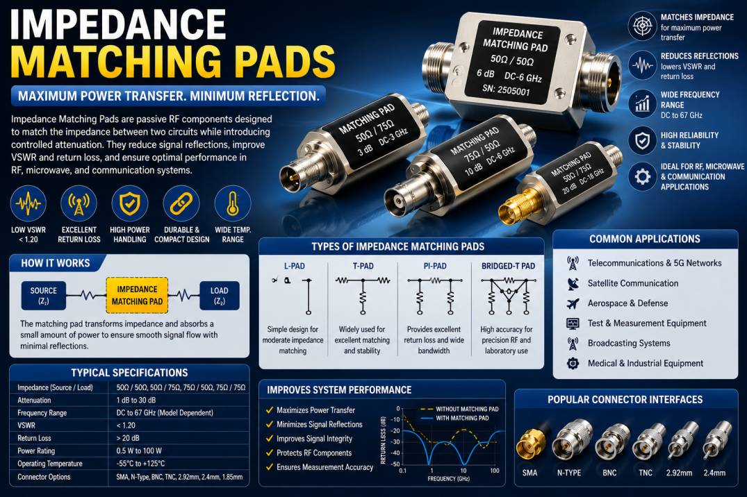
An Impedance Matching Pad is a passive resistive network specifically designed to match the impedance between two RF circuits while reducing signal reflections and maintaining controlled signal attenuation.
Unlike ordinary attenuators that simply reduce signal power, impedance matching pads are engineered to transform one impedance value into another. For example, they can connect a 75 Ohm system to a 50 Ohm system while maintaining excellent signal integrity.
Impedance Matching Pads are commonly used wherever different impedance systems must be interconnected without introducing excessive reflections or distortion.
How Do Impedance Matching Pads Work?
An Impedance Matching Pad operates using a precisely designed network of resistors that both attenuates the RF signal and transforms impedance between connected devices.
When an RF signal travels through a transmission line and encounters an impedance mismatch, part of the signal is reflected back toward the source. These reflections create standing waves, increase VSWR, reduce transmitted power, and negatively affect overall system performance.
An Impedance Matching Pad eliminates this mismatch by presenting the correct impedance to both the source and the load. The resistor network absorbs a small portion of the RF energy while allowing the remaining signal to pass with minimal distortion.
As a result, the system experiences:
- Lower signal reflections
- Improved power transfer
- Reduced VSWR
- Better return loss
- Higher measurement accuracy
- Enhanced signal stability
Why Impedance Matching Is Important
Proper impedance matching is one of the most important factors in RF engineering.
Without impedance matching:
- Signal reflections increase.
- Standing waves develop.
- Power transfer decreases.
- Amplifiers become unstable.
- Receivers experience reduced sensitivity.
- Test equipment produces inaccurate measurements.
- Communication quality deteriorates.
- RF components may overheat or become damaged.
Impedance Matching Pads solve these problems by creating smooth impedance transitions between different RF devices.
Construction of Impedance Matching Pads
Impedance Matching Pads consist of several precision components.
Precision Resistors
The resistors determine both the attenuation and impedance transformation.
High-stability thin-film resistors are commonly used because of their excellent frequency response and temperature stability.
RF Connector Interfaces
Matching pads are available with several connector options including:
- SMA
- N-Type
- BNC
- TNC
- 2.92 mm
- 2.4 mm
- 1.85 mm
- 7/16 DIN
- 4.3-10
Protective Housing
The housing protects internal components against environmental conditions while providing mechanical durability.
Materials include:
- Stainless steel
- Nickel-plated brass
- Aluminum alloy
Types of Impedance Matching Pads
Several resistor network configurations are used depending on the application.
L-Pad
The simplest impedance matching network.
Used for moderate impedance transformation.
Advantages:
- Low cost
- Compact design
- Easy implementation
T-Pad
A three-resistor configuration commonly used in RF systems.
Advantages:
- Excellent impedance matching
- Stable attenuation
- Wide frequency response
Pi-Pad
A three-resistor network shaped like the Greek letter Pi.
Widely used for:
- RF communication
- Microwave systems
- Precision measurements
Advantages:
- Excellent return loss
- Better impedance stability
- Wide operating bandwidth
Bridged-T Pad
Used where extremely accurate attenuation and impedance matching are required.
Often found in laboratory calibration equipment.
Technical Specifications
| Specification | Typical Value |
| Input Impedance | 50 Ohms |
| Output Impedance | 50, 75 Ohms |
| Frequency Range | DC to 67 GHz |
| Attenuation | 1–30 dB |
| Return Loss | Better than 20 dB |
| VSWR | Less than 1.20 |
| Power Rating | 0.5 W to 100 W |
| Operating Temperature | -55°C to +125°C |
| Connector Types | SMA, N-Type, BNC, TNC, 2.92 mm |
Common Impedance Conversion Values
| Source Impedance | Load Impedance | Typical Application |
| 50 Ω | 75 Ω | RF to Video Systems |
| 75 Ω | 50 Ω | CATV to RF Equipment |
| 50 Ω | 50 Ω | RF Signal Conditioning |
| 75 Ω | 75 Ω | Broadcast Systems |
Key Features of Impedance Matching Pads
- Precise impedance transformation
- Controlled signal attenuation
- Excellent return loss
- Low VSWR
- Stable RF performance
- Wide frequency compatibility
- Compact construction
- High reliability
- Excellent thermal stability
- Superior shielding
- Long service life
- Easy installation
Frequency Range
Impedance Matching Pads are available for numerous frequency bands.
Typical operating ranges include:
- DC to 1 GHz
- DC to 3 GHz
- DC to 6 GHz
- DC to 12 GHz
- DC to 18 GHz
- DC to 26.5 GHz
- DC to 40 GHz
- DC to 50 GHz
- DC to 67 GHz
Specialized versions support frequencies exceeding 110 GHz.
Applications of Impedance Matching Pads
Telecommunications
- Cellular base stations
- RF repeaters
- Wireless communication
- Network infrastructure
5G Networks
- Massive MIMO
- Small cells
- RF front-end modules
- Beamforming systems
Satellite Communication
- Ground stations
- Satellite transceivers
- VSAT systems
Aerospace
- Aircraft communication
- Navigation systems
- Avionics
Defense
- Radar systems
- Electronic warfare
- Secure communication
Broadcasting
- Television transmitters
- Radio broadcasting
- Signal distribution
Medical Equipment
- MRI systems
- RF diagnostic equipment
- Medical imaging
Test and Measurement
- Spectrum analyzers
- Network analyzers
- Signal generators
- RF calibration systems
Industrial Automation
- Wireless sensors
- Factory automation
- Industrial communication
Advantages of Impedance Matching Pads
- Maximum power transfer
- Reduced signal reflections
- Improved system efficiency
- Better return loss
- Lower VSWR
- Enhanced measurement accuracy
- Protection of RF equipment
- Stable frequency response
- Compact design
- Long operating life
- Minimal maintenance
- Cost-effective RF solution
Limitations of Impedance Matching Pads
- Introduce intentional insertion loss
- Fixed impedance transformation
- Limited power handling depending on model
- Cannot compensate for severe transmission line defects
- Incorrect selection reduces performance
How to Choose the Right Impedance Matching Pad
Before selecting an Impedance Matching Pad, evaluate the following:
- Source impedance
- Load impedance
- Operating frequency
- Required attenuation
- Power rating
- Connector compatibility
- Return loss
- VSWR
- Environmental conditions
- Mechanical size
Impedance Matching Pad vs RF Attenuator
| Feature | Impedance Matching Pad | RF Attenuator |
| Primary Function | Matches impedance | Reduces signal power |
| Impedance Conversion | Yes | No |
| Signal Attenuation | Controlled | Fixed or Variable |
| VSWR Improvement | Excellent | Moderate |
| Power Transfer | Optimized | Not optimized |
| Applications | RF Matching | Signal Level Reduction |
Best Practices for Installation
For optimal performance:
- Use the correct impedance values.
- Tighten connectors using the recommended torque.
- Avoid connector contamination.
- Keep cable lengths as short as possible.
- Inspect connectors periodically.
- Operate within the rated power limits.
- Maintain proper grounding.
Future Trends of Impedance Matching Pads
The demand for Impedance Matching Pads continues to grow with advancements in 5G, 6G, satellite communication, aerospace, autonomous vehicles, and high-frequency semiconductor testing. Modern designs focus on ultra-wideband performance, improved thermal management, lower insertion loss, compact packaging, and compatibility with millimeter-wave frequencies exceeding 100 GHz. As wireless systems become more complex, impedance matching pads will remain indispensable components for ensuring stable and efficient RF signal transmission.
Conclusion
Impedance Matching Pads are critical passive RF components that ensure maximum power transfer, minimize signal reflections, and maintain stable impedance throughout communication systems. Their ability to transform impedance while providing controlled attenuation makes them invaluable in telecommunications, aerospace, defense, satellite communication, medical equipment, industrial automation, broadcasting, and laboratory testing. Selecting the appropriate impedance, attenuation level, connector type, and power rating ensures reliable performance, improved signal integrity, and long-term system stability.
Frequently Asked Questions (FAQs)
1. What is an Impedance Matching Pad?
An Impedance Matching Pad is a passive RF component that matches the impedance between two circuits while introducing controlled attenuation to reduce signal reflections.
2. Why are Impedance Matching Pads used?
They are used to maximize power transfer, improve return loss, reduce VSWR, minimize reflections, and protect RF equipment from impedance mismatches.
3. What is the difference between an Impedance Matching Pad and an RF Attenuator?
An Impedance Matching Pad changes impedance while reducing signal power, whereas a standard RF attenuator primarily reduces signal power without changing impedance.
4. What impedance values are commonly used?
The most common impedance values are 50 Ohms and 75 Ohms.
5. What frequency range do Impedance Matching Pads support?
Depending on the model, they support frequencies from DC to 67 GHz, with specialized versions extending beyond 100 GHz.
6. What connector types are available?
Common connectors include SMA, N-Type, BNC, TNC, 2.92 mm, 2.4 mm, 1.85 mm, 7/16 DIN, and 4.3-10.
7. Where are Impedance Matching Pads used?
They are widely used in telecommunications, 5G networks, satellite communication, aerospace, defense, broadcasting, medical equipment, industrial automation, and RF laboratories.
8. How do I choose the right Impedance Matching Pad?
Consider source impedance, load impedance, operating frequency, attenuation, power rating, connector type, VSWR, return loss, and environmental conditions.
9. Can Impedance Matching Pads improve RF performance?
Yes. They reduce signal reflections, improve power transfer, lower VSWR, enhance return loss, and increase overall RF system stability.
10. Are Impedance Matching Pads suitable for high-power RF systems?
Yes. They are available in a wide range of power ratings, from low-power laboratory models to high-power versions designed for demanding RF and microwave applications.